Intel’s Ambitious Goal to Reclaim Semiconductor Leadership
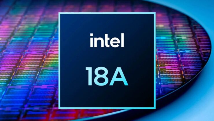
In a bold move to reassert its dominance in the semiconductor industry, Intel has unveiled its groundbreaking 18A manufacturing process. Spearheaded by CEO Pat Gelsinger, the company’s foundry division is undergoing significant restructuring to overcome past challenges. The introduction of the 18A process marks a pivotal advancement in this journey.
The Pinnacle of Intel’s Fabrication Nodes
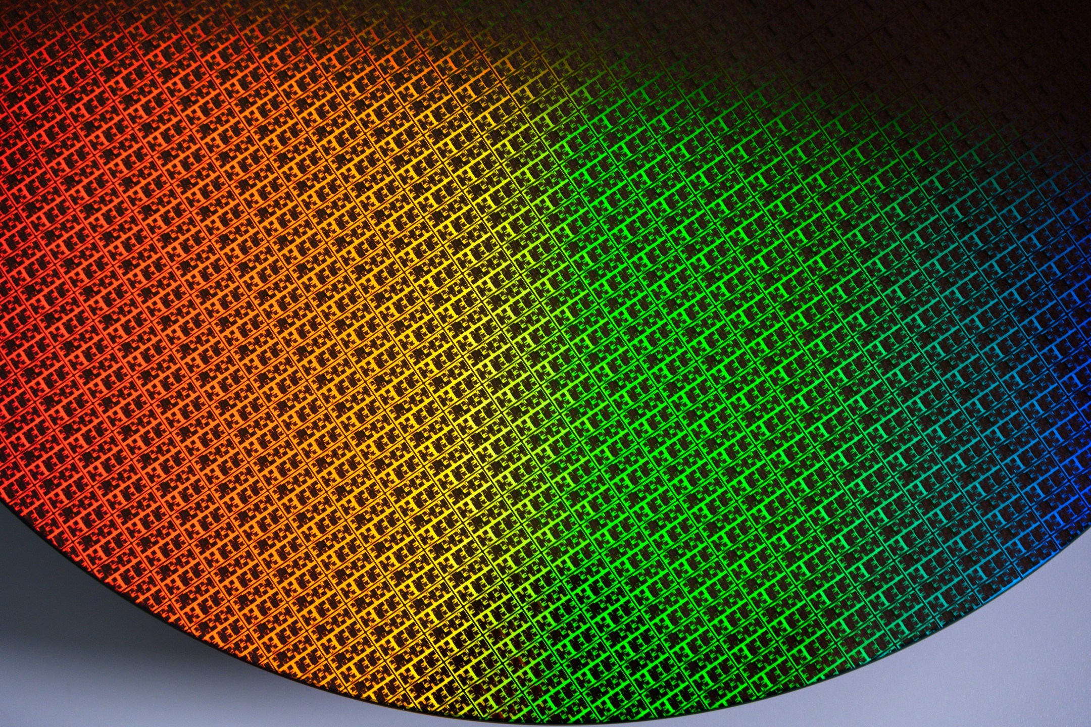
Presented at the 2025 VLSI Symposium, Intel’s latest fabrication technology is hailed as the most advanced node ever developed by the company. This next-generation process promises a density increase of more than 30 percent compared to the previous Intel 3 node.
Revolutionary Technologies: PowerVia and BSPDN
Central to the success of the 18A process are two innovative technologies: PowerVia and Backside Power Delivery Network (BSPDN). These breakthroughs allow for denser transistor packing and more efficient use of the chip’s front surface, crucial for high-density designs. In terms of PPA (Performance, Power, Area) metrics, the 18A process boasts 25 percent faster speeds and 36 percent lower power consumption at a 1.1V operating voltage, marking a significant improvement in both performance and energy efficiency.
Stability and Efficiency in Power Delivery
The information shared at the VLSI Symposium highlights the 18A process’s ability to maintain stable power delivery under high performance. PowerVia technology ensures direct power delivery to transistors from the backside, reducing complex connections on the chip’s front side and allowing for tighter cell placement. Cell library comparisons reveal that the 18A process matches, and in some instances surpasses, competitors in cell density and area efficiency. Notably, Intel’s 18A is competitive with TSMC’s N2 process in terms of SRAM density.
Anticipating the Future
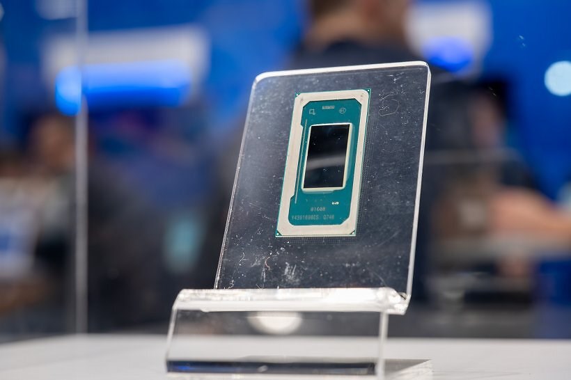
The 18A manufacturing process is set to debut in Intel’s Panther Lake SoCs and Xeon “Clearwater Forest” server processors later this year. Should Intel achieve the desired yield levels, products featuring this cutting-edge technology are expected to hit the market by 2026, potentially including offerings from external customers.