


The cutting-edge system developed by the company faces compatibility challenges with existing production infrastructures. Consequently, Substrate plans to reinvent its supply chain from the ground up. Aiming to offer their production as a service, they will establish their very own factory.

With the rapid advancement of integrated circuits, manufacturers now rely on advanced, costly lithography machines more than ever. Acquiring an ASML NXE:3800E EUV scanner, for instance, demands approximately $235 million, while the ASML EXE:5200B High-NA goes for $380 million. Such exponential costs significantly elevate both factory setup and chip production expenses.

Revolutionizing Advanced Chip Production
Projection insights from Substrate suggest foundational costs for modern factories might hit a staggering $50 billion by 2030. Consequently, chip production may become accessible only to financially robust corporations. However, Substrate’s groundbreaking ambition is to slash production costs per 300 mm wafer from $100,000 to $10,000.

Decoding X-ray Lithography
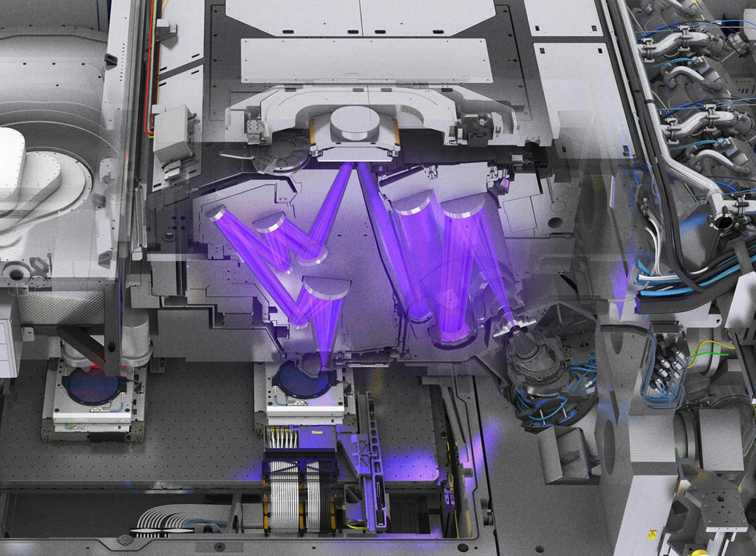
Substrate’s innovation involves a state-of-the-art particle accelerator, propelling electrons to nearly light speed. As these electrons traverse magnetic fields, they emit intense X-ray beams, described by the company as “billions of times brighter than the Sun.” This process allows for the precise patterning of chips.
The system uses direct writing, bypassing the need for reticles or masks. Though this method is research-effective, it’s yet to be optimized for mass production. Utilizing X-rays with wavelengths of 0.01 nm – 10 nm greatly refines structure production, notwithstanding the complexities in controlling such light.
Substrate’s recent achievement includes crafting high-precision patterns with a 12 nm critical dimension and 13 nm top-to-top spacing, outperforming current EUV technology resolution capabilities. Moreover, their set benchmarks in alignment accuracy and uniformity further promise unparalleled performance.
Overcoming technological hurdles
Numerous technical challenges await addressing: from beam sturdiness and optical responsiveness, to novel photoresist materials resistant to X-rays. Additionally, there’s the requirement for exact mirror production, X-ray prevention from damaging micro-components, achieving sub-1 nm alignment accuracy, and ensuring efficient mass production.
Given that ASML’s EUV technology took over a decade to transition from laboratory concept to production scale, Substrate might face a similar developmental trajectory. Their approach diverges from traditional models as they intend to produce chips within their own factories, valuing a self-sustained strategy for U.S. semiconductor independence. This dual-role might strain resources, yet success would potentially revolutionize the semiconductor sector, challenging ASML’s and TSMC’s dominance, and perhaps realigning global manufacturing powers.


Yorum Yap